Cim: Difference between revisions
No edit summary |
No edit summary |
||
| Line 99: | Line 99: | ||
UART1 - SAS + bootloader | UART1 - SAS + bootloader | ||
UART2 - ISM communication | UART2 - ISM communication | ||
0 and 2 are multiplexed | |||
I think in normal conditions all of them run at 9600 | |||
12V tx and rx on same line | |||
want to see signal? | |||
Revision as of 14:50, 27 July 2022
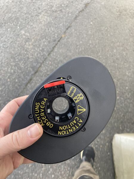
Saab 9-3 CIM Column Integrated Module
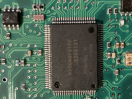
MCU: M306NAFGTFP
RAM: 10k
ROM: 256k
Starting it in bench
    ____________________________________________
   |    +B       PH PL +15                      |
   | 17 18 19 20 21 22 23 24 25                 |
   |                                            |
   |  1  2  3  4  5  6  7  8  9   11 12  14 15  |
   |+30    GND         GND                      |
   |____________________________________________|
PH P-bus CAN High
PL P-bus CAN Low
Power
12v to pin 1, 18 and 23, ground on pin 3 & 7
pin 18 is the "wakeup" signal to CIM from ISM, it's a switch that engages when a key is inserted
pin 23 is the "key in on position" signal from ISM
if 18 and 23 is not powered the CIM will not start broadcasting on the p-bus. unknown if it's listening with only +30 yet
I-bus
All 3 I-bus pinns are connected to each other(!??)
P-bus
Broadcasted Message id's
   0x0C1
   0x0C5
   0x180
   0x1F5
   0x380 audio RDS status?
   0x381
GlobalTIS binarys
Remove 20 first bytes from 176kb file to make all vector tables etc line up in IDA
Header
   5F 6E | 00 01 21 | 00 C3 7A E6 | 41 41 | 01 00 0D 00 00   | 00 02 BE 00                  |
   ????  | same in  | 12810982    |  AA   | write dest? same | 179712 size after 20b header |
   crc16?| all bins | module name |  rev  | in all bins      | same in all bins             |
CAN
CIM listens to 0x245 on p and i-bus and replies on 0x645
Memory layout
Dumping memory from CIM using $23 over GMLAN is possible for the following ranges
   0x100000 - 0x1003FF
   0x100400 - 0x1017FF
   0x200000 - 0x20001A
   0x800000 - 0x800110
0x8000A0 contains a power on counter
Serial dumping
MCU is ID locked, ID is currently unknown
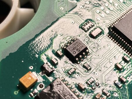
EEPROM
Type: 93LC66A-I
Packaging: SOP8
   CS connected to P50 CS0
   DI to P49 CS1
   DO to P39 RDY/CLKOUT
   SK/CLK to P51
   DC to GND
Other
H000004457
bojer: Side note on transponder - for cim to think it is valid key it needs to have isk locked AND protect write user pages (PWUP) flag on bojer: as in: page 3 first byte needs to be 0x96
chriva: Found what I wanted to know. If 0F_BE03 is not set to 0x8f it's simply not going to jump to the main firmware. As for how it knows where to enter the main firmware: That's a tribyte-address stored at 0F_BDED
chriva: The utility program is to be stored at EXACTLY address 0x614 and up. All those weird bytes finally made sense
uart2 goes to pin 17 of CIM (comm with ISM)
UART0 - SCL communication UART1 - SAS + bootloader UART2 - ISM communication 0 and 2 are multiplexed
I think in normal conditions all of them run at 9600 12V tx and rx on same line want to see signal?


